
Volume 50 Number 1 (2019.3)
Special Feature
Analysis Techniques to Evaluate the Next Generation Electronic Materials
Overview
Research Reports
-
2. Defect Detection in Semiconductor Materials by Luminescence Analysis
 (888kB)
pages 1-9
Keita Kataoka, Tetsuo Narita, Hiroko Iguchi, Masakazu Kanechika, Ken Hattori, Aishi Yamamoto and Tetsu Kachi

Cathodoluminescence (CL) and photoluminescence (PL) can sensitively detect crystal defects in semiconductors. Luminescence spectra contain important information on radiative defects and impurities. The relative concentration of nonradiative defects is evaluated through comparison with the total luminescence intensity. We use CL and PL to study three cases essential to semiconductor device research.
-
3. Local Atomic Structure Analysis of SiO2/SiC Interfaces Using X-ray Absorption Spectroscopy
(783kB)pages 11-17
Noritake Isomura, Takamasa Nonaka and Yukihiko Watanabe

Local atomic structure analysis of the interface between SiO2 and SiC is achieved by a combination of chemical-state-selective extended X-ray absorption fine structure (EXAFS) spectroscopy and a thinned SiO2 film sample. SiC- and SiO2-selective EXAFS measurements suggest the existence of carbon vacancy defects on the SiC side of the interface and a structure close to that of tridymite on the SiO2 side, respectively.
-
pages 19-26
Kayo Horibuchi, Satoshi Yamaguchi, Yasuji Kimoto, Koichi Nishikawa and Tetsu Kachi

The threading dislocations were investigated in a GaN substrate synthesized using a basic ammonothermal method and an epitaxial layer on the substrate using synchrotron radiation X-ray topography and transmission electron microscopy. A “helical dislocation” is reported, in which the threading dislocations are deformed by heat treatment of the substrate, a phenomenon observed for the first time in GaN crystals.
-
pages 27-37
Tetsu Ohsuna, Ritsuko Yaokawa and Hideyuki Nakano
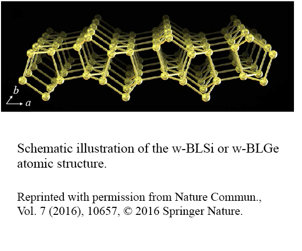
Two new 2D crystals of bilayer silicene and germanene were recently identified in the fluorinated Zintl-phase crystallites of CaSi2 and CaGe2, respectively. They have the same atomic structure, consisting of 4-, 5-, and 6-membered rings of Si/Ge atoms that form a wavy shape, and are denoted w-BLSi and w-BLGe, respectively.
-
pages 39-47
Hidehiko Kimura, Masanori Usui, Michiaki Kamiyama, Takashi Asada, Satoshi Yamaguchi, Daigo Setoyama and Toshikazu Satoh

Synchrotron radiation X-ray was applied to measure internal degradation behavior in intelligent power modules. The laminography measurements revealed improved fatigue property of nano-particle Cu bonding layer due to the unique microstructure. A developed spiral slits system enabled space-resolved diffraction measurement useful for internal stress evaluation. Those techniques will be a powerful tool for the reliability analysis of power modules.