
SiC and GaN are attracting attention as nextgeneration power device materials due to their high energy bandgaps and critical electric fields. Although GaN devices have difficulty handling large currents, such as they found in electric vehicle applications, GaN power devices are anticipated to reduce loss and costs more than SiC devices. We developed a p-type GaN layer burying technology, which we have successfully used to demonstrate the world's first vertical structure capable of carrying large currents. Applying GaN power devices in practice, however, will also require a high quality GaN substrate, gate insulator, and p-type GaN formed by ion implantation. In order to overcome these issues, we actively promote industry-academia collaborations, and will contribute to the promotion of greater electric vehicle use.
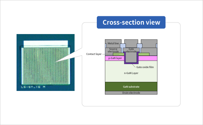
Structure of a prototype vertical GaN power device